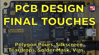
PCB Design Final Touches (Tips & Checklist) - Phil's Lab
Tips when finishing up a PCB design before manufacturing (polygon pours, solder mask, silkscreen, teardrops, etc.). PCBs by PCBWay https://www.pcbway.com
[SUPPORT]
Hardware design courses: https://phils-lab-shop.fedevel.education
Course content: https://www.phils-lab.net/courses
Patreon: / phils94
Free trial of Altium Designer: https://www.altium.com/yt/philslab
Free search engine for the best quality components from Octopart: https://octopart.com/
Learn about Altium 365, the electronics product design platform that unites PCB design, MCAD, data management, and teamwork: https://www.altium.com/altium-365
[GIT]
https://www.github.com/pms67
[SOCIAL]
Instagram: / philslabyt
[LINKS]
Stitching Vias: https://resources.altium.com/p/everyt...
Fiducials: https://resources.altium.com/p/are-fi...
[TIMESTAMPS]
00:00 Introduction
01:50 PCBWay
02:34 Altium Designer Free Trial
03:24 Board Overview
04:57 #1 Schematic & PCB Synchronisation
05:30 #2 Polygon Pour Clearance
06:43 #3 Thermal/Copper Balance
07:10 #4 Stitching
07:57 #5 Polygon Pour Clean-Up
09:12 #6 Plane Voiding
10:59 #7 Non-Functional Pads
12:52 #8 Teardrops
14:48 #9 Transfer Vias
17:02 #10 Missing Plating
18:08 #11 Fiducial Markers
20:14 #12 Silkscreen
22:38 #13 Solder Mask
26:59 #14 Mechanical Checks
28:40 #15 Polygon Repours & Pour Order
29:51 #16 Design Rules & Routing Completion
31:49 #17 Gerber Viewer
33:40 #18 Footprint Checks
36:37 #19 Manufacturing/Assembly Info
37:45 Outro