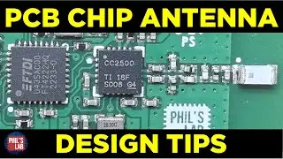
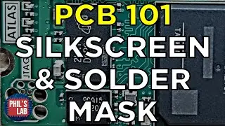
PCB Silkscreen & Solder Mask 101 - Phil's Lab
Basics, tips and tricks for working with silkscreen and solder mask in PCB designs. PCBs by PCBWay https://www.pcbway.com
[SUPPORT]
Hardware design courses: https://phils-lab-shop.fedevel.education
Course content: https://www.phils-lab.net/courses
Patreon: / phils94
Free trial of Altium Designer: https://www.altium.com/yt/philslab
Free search engine for the best quality components from Octopart: https://octopart.com/
Learn about Altium 365, the electronics product design platform that unites PCB design, MCAD, data management, and teamwork: https://www.altium.com/altium-365
[GIT]
https://www.github.com/pms67
[SOCIAL]
Instagram: / philslabyt
[LINKS]
Vias 101: • PCB Vias 101 - Phil's Lab #77
Traces 101: • PCB Traces 101 - Phil's Lab #112
Silkscreen: https://www.pcbway.com/pcb_prototype/...
https://resources.altium.com/p/your-g...
Solder Mask: https://www.pcbway.com/pcb_prototype/...
https://www.pcbway.com/blog/Engineeri...
[TIMESTAMPS]
00:00 Introduction
03:02 PCBWay
03:44 Altium Designer Free Trial
04:35 Silkscreen
08:39 Silkscreen Sizing
11:02 Silkscreen Placement & Clearance
14:17 Silkscreen Date Code
15:04 Silkscreen Tip for Dense Designs
15:40 Solder Mask
18:54 Solder Mask Expansion
20:13 Solder Mask Colour Considerations
21:16 Solder Mask Slivers (Bridges)
25:05 Tented Vias
26:15 (Non) Solder Mask Defined Pads
27:55 Outro