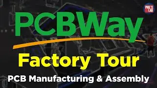
How PCBs are Manufactured & Assembled (PCBWay Factory Tour) - Phil's Lab
See how PCBs are made and assembled in the huge PCBWay factory in Shenzhen, China! https://www.pcbway.com
[SUPPORT]
Hardware design courses: https://phils-lab-shop.fedevel.education
Course content: https://www.phils-lab.net/courses
Patreon: / phils94
[GIT]
https://github.com/pms67
[SOCIAL]
Instagram: / philslabyt
[LINKS]
Manufacturing process: https://www.pcbway.com/pcb-service.html
SMT assembly process: https://www.pcbway.com/assembly-proce...
[TIMESTAMPS]
00:00 Intro
01:31 Fabrication Data Generation
02:37 Panel Cutting
03:17 Inner Layers
04:18 Lay-Up
05:13 Pre-Pregs & Copper Foils
06:20 Lamination
07:55 Drilling
09:10 PTH & Electroless Copper Deposition
10:13 Imaging Outer Layers
11:54 Plating
13:15 Etching
14:38 Automatic Optical Inspection (AOI)
15:29 Solder Mask
18:24 Surface Finish
19:50 Silkscreen
20:50 Outline
21:44 E-Test & Final Inspection
23:33 Assembly Process & Incoming Quality Control
25:30 Stencil, Solder Paste, Pick 'n' Place
28:01 Reflow & Inspection
29:28 Through-Hole Assembly & Packaging
31:06 Outro


![OSU! [supercell - Hero Kowari's Insane] 4.42 FC S](https://images.videosashka.com/watch/l4DQHYtqzqY)