EEVblog
What difference does a 4 layer PCB make to EMC radiated emissions compared to an identical 2 layer PCB? And why?
Dave does H-Field near-field probe testing on two otherwise identical PCB's.
Electromagnetic waves and the difference between near field and far field, and H-Field and E-field probes and wave impedance is also explained.
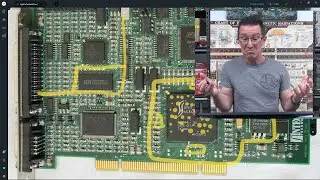
The PCB layout is then examined to look at loop area and by-passing and what effect this has.
Forum: http://www.eevblog.com/forum/blog/eev...
https://gigatron.io/
Designing the 4 layer board: • KiCAD PCB Design
Bypass capacitor Visualised: • EEVblog #1085 - Bypass Capacitors Vis...
PCB Power Plan Capacitance: • EEVblog #1117 - PCB Power Plane Capac...
Bitcoin Donations: 38y7DE8HEHNj8fGDtUr4PkCn9nWxiorvvy
Litecoin: ML7oQokTwB38bgzzjLDbRV97HKAHuwRfHA
Ethereum: 0x11AceA38DCA9DbFfB4F35f3F746af65F9dED28ce
EEVblog Main Web Site: http://www.eevblog.com
The 2nd EEVblog Channel: / eevblog2
Support the EEVblog through Patreon!
/ eevblog
AliExpress Affiliate: http://s.click.aliexpress.com/e/c2LRpe8g
Buy anything through that link and Dave gets a commission at no cost to you.
Stuff I recommend:
https://kit.com/EEVblog/
Donate With Bitcoin & Other Crypto Currencies!
https://www.eevblog.com/crypto-currency/
T-Shirts: http://teespring.com/stores/eevblog
Likecoin – Coins for Likes: https://likecoin.pro/@eevblog/dil9/hcq3
#PCBdesign #PCBdesign #EMC


